Tutorials
At EOSAM 2025, as in previous EOSAM conferences, in addition to the conference program including contributed and invited speakers, we wish to provide an additional benefit to all registered attendees in the form of tutorials covering Topical Meeting (TOM) and Focused session topics. These tutorials will take place on Sunday, 24 August 2025.
Participation in these tutorials is free for all registered conference attendees, but pre-registration is required for each tutorial. Registration will open by April 2025.

Sylvain Gigan
Sorbonne Université, Ecole Normale Supérieure, France
Photonics for AI : coming of age?
Photonics is an ideal technology for low-energy and ultrafast information processing, and photonic computing is currently seeing a surge of interest, with exciting perspectives. In Machine Learning, optics is naturally well suited to implement a layer of a neural network, via either in integrated or free-space approaches. However, most optical machine learning have been until recently limited to modest dimensions, single-layer or relatively shallow artificial neural layer networks, and to relatively simple ML tasks. This tutorial will present a broad overview of the current state of the art, and discuss some of the key challenges ahead. It will show how multiple scattering of light allows performing optically an interesting operation for machine learning : large scale random matrix multiplication. Their application to various tasks will be presneted and how we can extend this concept beyond single layers operations, and to modern machine learning tasks.
Sylvain's tutorial will concern at least the following TOMs and Sessions:
About the Speaker
Sylvain Gigan is Professor of Physics at Sorbonne Université in Paris, and group leader in Laboratoire Kastler-Brossel, at Ecole Normale Supérieure (ENS, Paris). His research interests focuses on light propagation in complex media, and range from fundamental investigations, biomedical imaging, computational imaging, signal processing, to quantum information. He is also the cofounder of a spin-off: LightOn (www.lighton.ai) developing optical computing solutions for machine learning. He is the recipient of two ERC grants in 2011 and 2017.

Julius Muschaweck
JMO GmbH, Germany
Introduction to Colorimetry
This course introduces the physiology of human color vision, the common CIE color spaces, color difference metrics and color rendering metrics.
An easy-to-grasp, intuitive visualization of additive color mixing in the common CIE 1931 XYZ color space is explained.
Practical examples of colorimetric computations are presented, interactively with a freeware GUI program, and programmatically, using free, open source Matlab and Python libraries.
Julius's tutorial will concern at least the following TOMs:
Visit https://www.jmoptics.de/
About the Speaker
Julius Muschaweck, a German physicist, has been working on optical design for illumination for almost thirty years.
He was co-founder and CEO of OEC, an optical engineering service which pioneered freeform optics for illumination.
Later, at OSRAM, where he held the position of Senior Principal Key Expert, he coordinated the over 100 optical designers within OSRAM world-wide.
He then joined ARRI, the leading movie camera and lamp head maker, as Principal Optical Scientist.
Julius Muschaweck now works as an independent consultant, providing illumination optics solutions to industry clients, teaching courses on illumination optics, and writing about the subject.
He is the author of over 25 scientific papers and the inventor of over 50 patent applications.
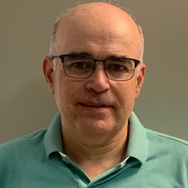
Ignacio Moreno
Universidad Miguel Hernández, Spain
Spatial Light Modulators
Spatial Light Modulators (SLM) have become common devices in Optics in Photonics laboratories. They are high-resolution micro-displays useful for displaying reconfigurable intensity, phase or polarization spatial patterns, thus being key components in adaptive optics and programmable diffractive optics. This tutorial will present the fundamentals of SLM technology, their modulation configurations and techniques for their characterization. The tutorial will also cover the design of diffractive optical elements and its realization with SLMs.
The tutorial will include a practical demonstration from the company Holoeye Photonics (Home - HOLOEYE Photonics AG), one of the major suppliers of SLMs.
Ignacio's tutorial will concern at least the following TOMs and Sessions:
- Face2Phase
- TOM: Adaptive and Freeform Optics
- TOM: Applications of Optics and Photonics
- FS: Visual Optics and Imaging
About the Speaker
Ignacio Moreno is Full Professor of Optics at Universidad Miguel Hernández of Elche, where he leads the TecnOpto Lab. He has extensive experience in the field of liquid crystal spatial light modulators, and their application in diffractive optics and polarization optics, being coauthor of more than 180 articles published in peer reviewed journals. He is Fellow member of SPIE and OPTICA. For 10 years he was associate editor of the journal Optical Engineering for the subject of optoelectronic displays, where he leaded two special issues devoted to “Liquid Crystals for Photonics” (2011), and to “Spatial Light Modulators: Devices & Applications” (2019).

Martijn Anthonissen
Eindhoven University of Technology, The Netherlands
Computational Illumination Optics
When it gets dark and we switch on the lights, we want to be surrounded by comfortable light. The light source is typically an LED that is combined with reflectors and lenses to send the light where you want it to be. Given the light distribution of the source and the desired target distribution, what is the optical system (reflector, lens or a combination) that does the job? That is the question we need to answer!
This field is freeform design and it is used for, e.g., solar energy concentration, car lights, luminaires and street lights. The optical surfaces are referred to as freeform since they do not have any symmetries. To find the optical components there are basically two approaches: direct methods and inverse methods.
In direct methods an optical component is designed in a CAD tool and the target light distribution is calculated using ray tracing. We follow many rays from the source to the target using the laws of optics (Snell’s law, law of reflection) and determine the light distribution at the target. If the obtained light distribution differs from the desired one, the CAD geometry is adjusted and a new light distribution is calculated. Because of the iterations, this is typically a slow process.
Instead, we treat this as an inverse problem and directly find the shape of the required optical components. A partial differential equation can be derived that describes the shape of the lens or reflector. Our mathematical model is based on the principles of geometrical optics, formulated in terms of the optical map connecting source and target domain, and energy conservation. This leads to a fully nonlinear partial differential equation of Monge-Ampère type.
In the tutorial we outline how to model optical systems mathematically (Hamiltonian optics, Hamilton’s characteristic functions, reflector and lens equations, optimal transport) and how to compute numerical solutions of the resulting equations (iterative least-squares method for partial differential equations of Monge-Ampère type).
Martijn's tutorial will concern at least the following TOM:
About the Speaker
Martijn Anthonissen works at Eindhoven University of Technology in the Computational Illumination Optics group. This is one of the few mathematics groups worldwide working on optical design problems from illumination optics. The team has a healthy portfolio of PhD positions and close collaborations with industrial partners. The research focuses on nonimaging freeform optics, imaging optics and improved direct methods.

Hugo Cramer
ASML, The Netherlands
Scatterometry in the Semiconductor Industry
Scatterometry is an optical measurement technique used in the semiconductor industry to support tight control of lithography and patterning processes. This tutorial will explain the working principles, hardware implementations, and parameter inference methods. Various examples will show the application and value of scatterometry in semiconductor manufacturing.
Hugo's tutorial will concern at least the following TOM:
About the Speaker
Hugo Cramer is Senior Systems Architect for metrology applications at ASML, The Netherlands. Hugo has been working in the field of semiconductor metrology and applications for over 20 years. He is a co- author of several patents and publications. Since 2007 he has been teaching a courses on Scatterometry and Applications at the yearly SPIE Advanced Lithography and Patterning symposium.

Simon Horsley
University of Exeter, United Kingdom
Topology, Waves, and the Refractive Index
This tutorial is divided into two parts: the first examines the application of topology to problems in wave physics. The origins of the Chern number are reviewed, where it is shown that this counts the number of critical points of a complex tangent vector field on the surface. We then show that this quantity arises naturally when calculating the dispersion of modes in any linear system.
The second part offers a physical interpretation for the Chern number, based on the idea that the critical points which it records can be understood as points where the refractive index vanishes. Using the theory of crystal optics, we show that when the refractive index vanishes in a complex valued direction, the wave is forced to circulate in only one sense, and this is the origin of the one-way propagation of topological interface states.
Simon's tutorial will concern at least the following TOM:
About the Speaker
Simon Horsley is an Associate Professor of Theoretical Physics at the University of Exeter, in the peaceful county of Devon in the UK. He is currently working on problems in the theory of wave propagation in time-varying materials. However, he recently completed an 8 year Royal Society and TATA University Research Fellowship, which gave him time to do things like writing tutorials about topology.

James Blakesley
National Physical Laboratory, United Kingdom
Applications of Digital Illumination in Metrology for Semiconductors and Photovoltaics
Digital illumination (DI), also known as Digital Light Processing (DLP), is the use of digital micromirror devices coupled to incoherent light sources to control illumination in space and time. In metrology, it presents opportunities to overcome many challenges of traditional illumination optics and introduces new concepts in measurement and characterisation.
This tutorial will introduce the use of DI for measurement and characterisation, illustrated with examples from the field of standards and metrology for photovoltaics and semiconductors. These include measurements of linearity, angular response, spectral response, operando functional imaging, hyperspectral and time-resolved photoluminescence imaging.
It will provide an introduction to the complementary concepts of spatial multiplexing (single-pixel imaging), compressing sensing and regularisation for image and spectrum reconstruction, and calibration and traceability. We will also discuss some of the challenges of the applications, such as stray light, dynamic range and computational efficiency.
James's tutorial will concern at least the following TOM:
About the Speaker
James Blakesley is a Principal Scientist and Science Area Leader for Electronic and Magnetic Materials at the National Physical Laboratory, the UK’s National Metrology Institute. His research work focuses on the development of standards and new characterisation methods for photovoltaics and semiconductor devices. His team works with industry and academic partners to overcome challenges with scale-up, commercialisation and application of semiconductor technologies.

Qingfeng Li
Thorlabs GmbH, Germany
Thorlabs Quantum Optics Kit
Thorlabs’ educational product line is designed to inspire students and educators by providing hands-on access to experiments in optics and photonics. This tutorial introduces the Quantum Optics Educational Kit, a versatile platform that enables the exploration of quantum phenomena using single and entangled photons. Participants will learn how to characterize a heralded single-photon source and use coincidence counting techniques. The session will also cover the Polarization-Entanglement Add-On, which extends the core kit for experiments involving Polarization-Entangled photon pairs. We will explain how polarization-entangled pairs can be used to measure the violation of Bell’s inequality, and the tutorial will conclude with a discussion of further experiments possible with the kit.
Qingfeng's tutorial will concern at least the following TOM:
About the Speaker
Qingfeng Li has been working in the field of optics and photonics for over a decade. He is a co- author of several publications and patents, particularly in the area of ultrashort pulse laser. Currently, he serves as an Academic Sales Engineer at Thorlabs GmbH in Germany, where he supports academic institutions across Europe in implementing photonics education and research solutions.
Thorlabs advances scientific innovation through the design and manufacture of photonics components, instruments, and systems. Its Discovery line of educational kits promotes hands-on learning in physics and photonics—from classic experiments to quantum optics—offered at the cost of the included components, with free educational materials and dedicated technical support.

Sara Nocentini
National Institute of Metrological Research, European Laboratory of Nonlinear Spectroscopy, Italy
3D printing of polymers at the nanoscale for advanced optics and photonics
Two-Photon Lithography (TPL), with its sub-diffraction resolution and versatility across 3D geometries and polymeric materials, has been beneficial in the development of 3D functional optic and photonic structures. These features have opened to several micro-optics and photonic structures such as photonic crystals, micro-lenses, diffractive optical elements and integrated circuits with a growing interest in new functional materials to be integrated into photonic chips.
This tutorial will introduce the fundamental principles of TPL and its crucial applications in photonics. While throughput limitations have been a challenge, recent technological advances are pushing its printing speed boundary by multi-foci printing and holographic approaches. Moreover, two-step absorption 3D laser nanoprinting using compact continuous-wave (cw) lasers and multi-focus parallelization offers a promising alternative.
Building upon these lithographic advancements, a key research direction focuses on developing functional materials that can serve as essential building blocks for realizing novel optical functions on integrated photonic chips, thereby enriching the field of polymer photonics.
Sara's tutorial will concern the following TOMs:
- TOM: Adaptive and Freeform Optics
- TOM: Nanophotonics
- TOM: Optical Materials
- TOM: Applications of Optics and Photonics
About the Speaker
Sara Nocentini is a researcher at the National Institute of Metrological Research in Italy and affiliated researcher to the European Laboratory of Nonlinear Spectroscopy in Florence.
Her research interests focuses on polymer photonics with a special focus on responsive liquid crystalline based materials and their nanopatterning via two-photon lithography. She is also working on smart materials for micro-robotics and cyber physical unclonable functions. She is author of more than 25 scientific article and the PI of an ERC Stg since 2025.
